A Large Digital Price Display for Precious Metals - Forex.
- Nima IS
- Jul 10, 2022
- 21 min read
Updated: Nov 3, 2022

This was a very interesting project back then when I was 19. It looks simple to me today, but I had worked on it for nearly 4 months from start to finish. The design was very modular as there was one microcontroller on a motherboard that could connect to up to 50 different price modules! Yes that’s right! 50 prices! each with 5 to 9 digits! The display would save all of the digits in case of a power outage too! It had a remote control for setting the digits, Power and Animation Mode.
In the model you see above, it’s only showing 4 prices. This is because this was a sample product that I used to show to clients. But to show more prices, all you had to do was to install more display modules, change the code slightly, install a repeater chip for the data line to repeat the signal between the modules to keep it strong, and it would handle more or less prices for customer x or y. Without the need to change the PCB modules or the circuitry in general.
The design was limited to 50 prices per microcontroller chip, because the chip used in this project (PIC16F877a) had a 256byte EEPROM memory. That means if we used one byte for each digit (inefficient yes. but for the sake of coding it easily), then 5 digits x 51 prices = 255 bytes. So we’d have another byte left (the 256th byte) for saving the configuration settings and others… . Using the same display module for all prices would greatly reduce the PCB manufacturing cost as well!
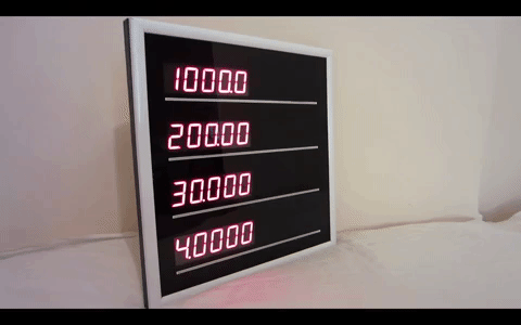
You can see the animation with prices in the gif above. This was done to attract customer’s attention to the prices shown. You could exit this mode simply by pressing any of 4 buttons on the remote control.
It was the first serious project I did to learn about PCB & product design as well as coding microcontrollers. By serious I mean market-ready. The coding was simple! and yet it was a valuable product because the market for Forex and precious metals was quite turbulent back in Iran and the prices could fluctuate greatly several times a day. Unfortunately, I guess that’s still the case in 2018… .
In this blog, we will talk about:
1. The Main features of This Display.
2. What’s inside?
3. What’s on the outside?
4. How does it operate?
5. Circuitry and PCB Design?
6. What’s In the Code?
7. Final Words.
1. The Main Features of This Display:
One display (microcontroller) can handle up to 50 prices or more thanks to this modular design.
RF Remote control with 4 easy to set buttons for setting the prices quickly.
Saving all of the prices on EEPROM memory for making it immune to power outages.
Supports up to 5 digits or more/less depending on the display module installed.
The display has a fully modular design that makes it great for expansion to suit customer needs. Without making any changes to the overall design and even after the display is produced/sold.
There are no stickers on the display itself making cleaning very easy and adding to its stylish looks.
Different sizes and colors of 7-segment display could be installed without changing the overall design.
It’s firmware could be updated through the ICSP connector without having to open the display.
Runs on 9v DC and can be turned off with the remote control.
Supports both Common Anode and Common Cathode 7-segment displays during production.
2. What’s inside?
Inside this Display is made of 2 main parts. One is the motherboard that controls all of the display modules and the other one is of course the display module(s).
Let’s start with the display modules:
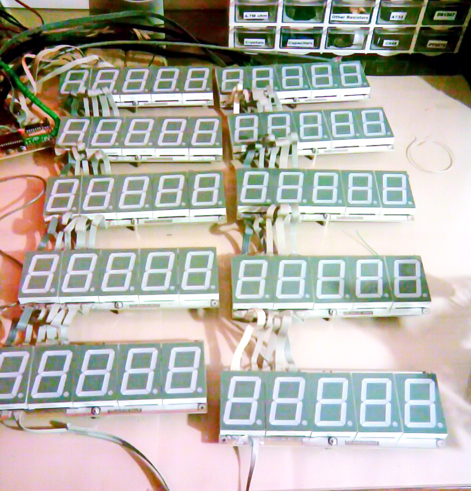
Yes, that’s a lot of digits. I know. What you’re looking at above is a good example of how easily this display can be scaled. that’s a 10-price display. Each digit has it’s own CD4543 driver chip at the back of the PCB:
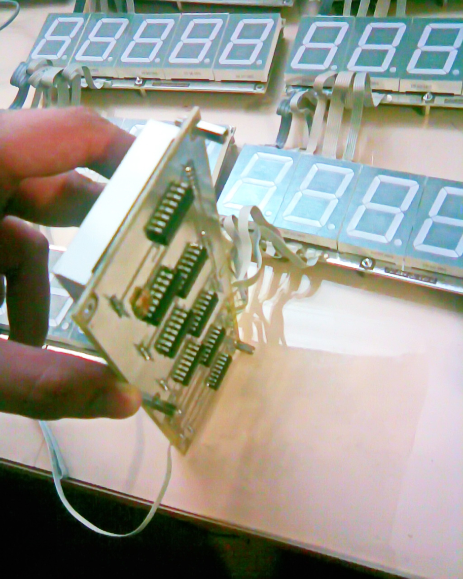
You can see that there’s a CD4543 driver chip installed behind each 7-segment. And a few more chips. 3 chips to be exact. One of the chips is a CD4017 that is in charge of the opening the latch of the driver chips (CD4543) so then our microcontroller can write a digit into the driver chip through the shared BCD (Binary Coded Decimal) line between all digits and display modules. This is a configuration that I used when making a large digital clock as well. It made the design very modular and easy.
OK. so what about the other two chips other than the CD4017 and the CD4543s? One of them is a transistor array and the other one is another CD4017. Why another CD4017 again? well because it’s cheap and useful chip! I used it to show the decimal on the 7-segments. There’s only one decimal in every price. So one CD4017 will do for each display module. But what if I’m using a common anode 7-segment? well that’s when the transistor array comes into play to invert the output of our CD4017.
OK, the displays are all fine and well. How about the motherboard module? Sure, let’s have a look at that too:
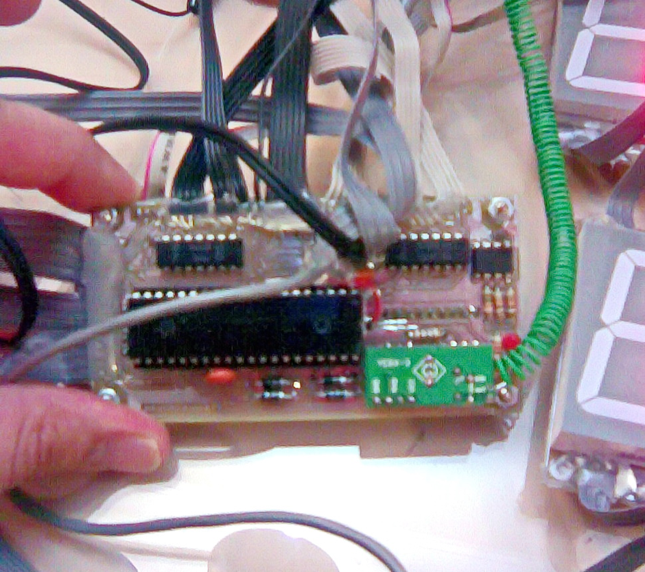
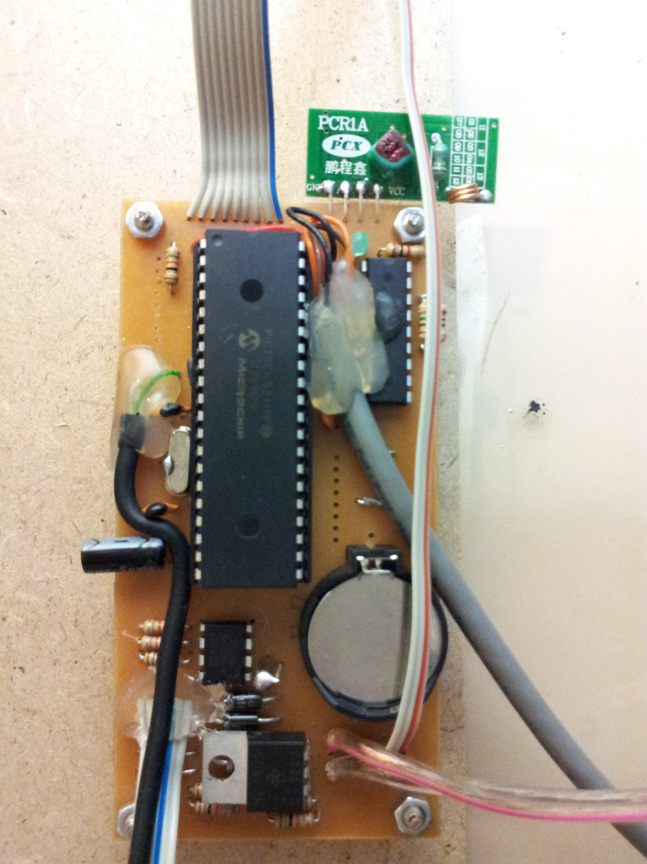
This is the first version of the motherboard module which is a double-sided board. The second version of the board was a single sided board in which was simpler but had the same components. This board houses the main microcontroller (PIC16F877a), the RF module and all the other bells and whistles necessary to make this display tick (the RF decoder chip, crystal chip and etc). We will discuss them in more detail when talking about the PCB design.
Lastly, there was a buttons modules as well which was located at the right hand corner of the price display which is simple and self explanatory:

There’s a common wire (GND) that is connected to one of the legs of each button. And each button has it’s own wire on the other leg. Therefore, there are 5 wires in total going to this module and the microcontroller chip will scan 4 wires simultaneously (half a port). That is the minimum amount of wires that I could use to read the buttons.
3. What’s on the outside?
The outside of this display was quite modest and simple as you can see below:

You could write the name of the item on the right hand side and show the price on the left hand side. But since this display’s design was very versatile, it could have a different look according to the customer’s requirements. The name of the items for instance, could be written on top or bottom of the digital price. Heck, there was one model of this display that included a clock as well:
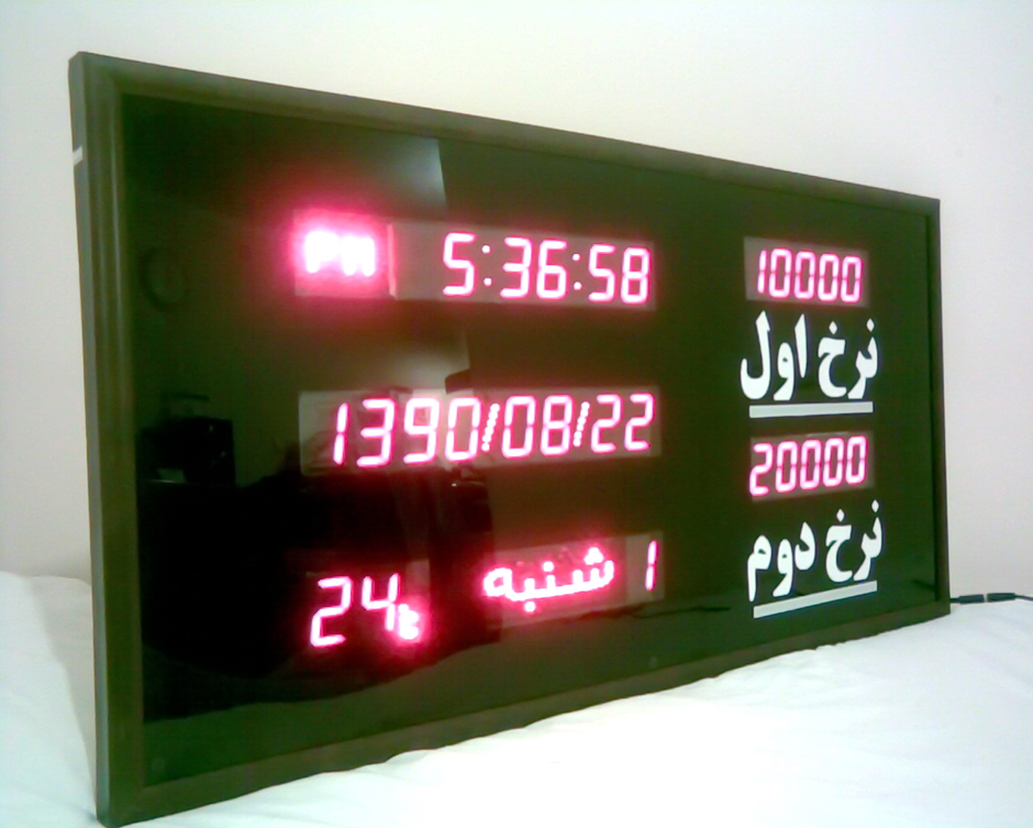
The model you see above uses one PIC micrcontroller chip (PIC16F877A) to show both prices and clock/date information. It’s a Hybrid version that combines the price display project with the clock project in which I did a year later. I had made the price displays, and I thought combining with a clock would make it an even more attractive product.
The model shown above can show time in AM/PM format. Persian Date, Persian weekdays and room temperature as well as the prices of 2 items. Thanks to it’s modularity (the PCB design), it could show up to 50 prices and the clock using the same microcontroller. You can read more about the clock project here.
This model operated with a remote control and used 4 buttons to control the settings.

You might have seen this picture in my previous blog. That is because both the price display and clock display used the same interface to configure their settings. They both used 9v to operate and had the same type of remote control and back panel with 4 buttons on it.
Here, you can see the ICSP socket which allows this display to have it’s firmware upgraded without having to open the panel at all. This made development quite easy for me actually. I had produced the panel before the firmware was final. I then kept updating the firmware until it was what I wanted it to be.
4. How does it operate?
Setting of prices for this display was quick and easy. There were only 4 buttons. Up, Down, Set and Select as you can see below:
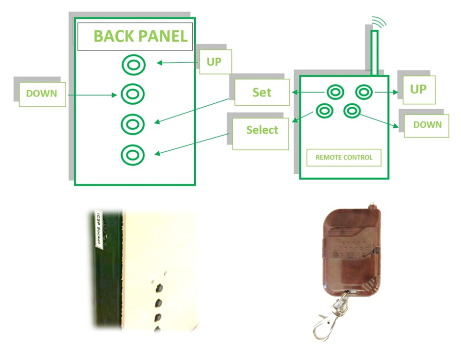
Setting up the prices was very easy. All you had to do was to press “SELECT” to see the selected price blink. you could then press “SELECT” to go to the next price and do a loop on all prices or press “SET” on a price that you wish to set so then you can change the value. In the SET mode, pressing “UP” and “DOWN” would change the value of the digit and pressing “SET” again would go to the next digit.
This way, you didn’t have to set all prices if you wished to make a change in only one of the prices. It was easy and you could simply choose (SELECT) the price you wished to modify, make the changes and press select to exit.
Unfortunately, I don’t have a video of how this setting could be done. and all of the units were sold so I can’t make a gif… but I think you get the idea. :)
5. Circuitry and PCB Design?
There are two types of PCB modules in this design and we will cover them separately so it’s easier to understand.
- Type one is the motherboard which comes in a double sided and single sided version with the same function.
- Type two is the display modules which come in a few different sizes for smaller and larger 7-segments but have the same circuitry design.
The circuitry and PCB design of this project is quite similar to another project that I finished a year later after this one. That project was a fully functional clock that would use the same motherboard and overall design configuration (how the modules connect to each other).
THE MOTHERBOARD MODULE
The motherboard in this design includes only a few components housed in a single board. It includes a PIC16F877a Micrcontroller chip that runs all of the program, A decoder chip that decodes the incoming signal from the remote control, A receiver module that receives the 315Mhz RF signals from the remote and finally a good old LM7805 regulator that helps to provide a clean 5V for the operation of everything on this board.
This motherboard design came in 2 versions and both of the versions could be used for either the clock project or the price display. If you wonder why I’ve tried to use one module for so many different things, it is because you can get very good discounts in the PCB manufacturing market if you order more PCBs of the same kind. So using the same motherboard for both designs would make sense. This is a strategy that large MNCs use as well. They make a great product and many other products that are similar to this with less functions. Then, they will market all of them together. So you might buy the product that doesn’t have all of the functions but is still a good product. You open the unit, and see that there’re many components missing. That is because the high end model of the said unit and the lower end model use the same PCB.
This way, the manufacturer can cut their cost and produce the same PCB for all off the different models in one range of products.
Let’s have a look at the schematic and PCB of this board:


You can see the Schematic and PCB of the first design. This is basically the brain of the project where all the code runs. One PIC16F877a takes care of it all. There are some extra components on the schematic that aren’t used in this project. Components such as the DS1307 Clock chip that wouldn’t do anything on a price display or a button cell battery that would be used to keep the same chip active. That is because I had considered to use this PCB for the clock project and then decided to proceed with the price display first. So when installing this motherboard into a price display, I just wouldn’t solder the clock chip or any other component that wasn’t necessary. And the same PCB would do.
I should also mention that the first PCB Design of this motherboard is unnecessarily complicated. I managed to reduce the number of jumpers (Via) to just a few by just doing a better job at the placement of these components. Put the components that share a bus with each other next to each other with the right alignment and group other components together similarly. So the second version became a single-sided board!
So let’s have a look at the second version of this PCB and you’ll see what I mean:
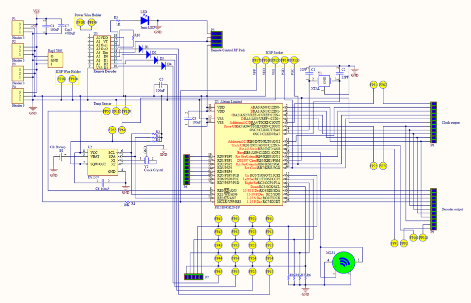
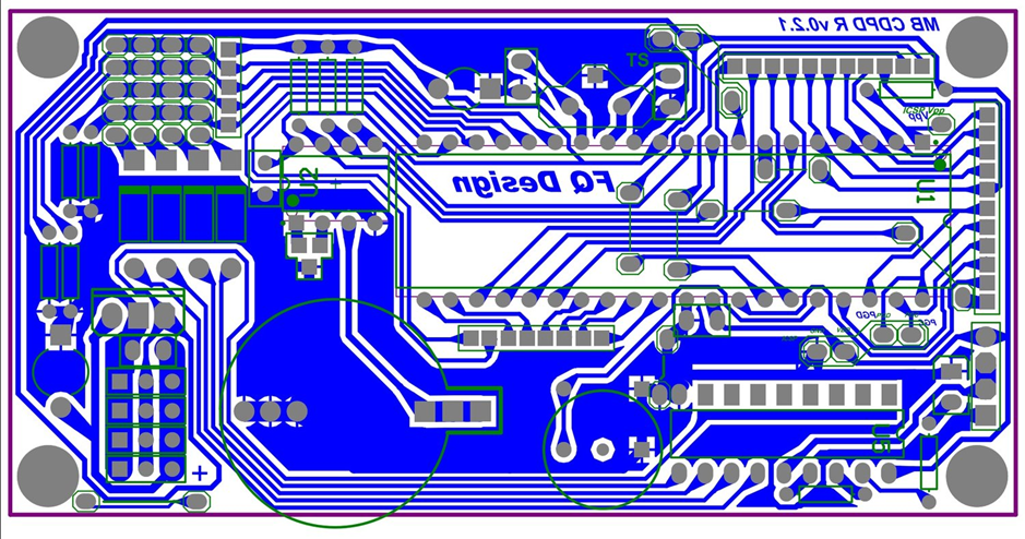
You can download the Schematic and PCB files from the links above. As you’ve noticed the PCB of the second motherboard looks much simpler and there is a GND that is covering most of the board. That will help to reduce the noise from outside that the board would receive to a small extent.
Speaking of noise reduction, there is another essential component that you should probably use for all of your microcontroller projects. That would be a 100nf capacitor right at the power input of your microcontroller. That would help to reduce the high frequency noises that usually mess up the operation of your microcontroller and cause it to restart (because of the watchdog). These noises can be caused by turning on the AC in your room or using the igniter that produces sparks to turn on your gas stove and etc.
That capacitor can illuminate those problems. A 100uF or higher capacitor would be necessary to fill the cap for short power disruptions in the realm of a few miliseconds. So 100uF and 100nF pair of capacitors in parallel are quite essential for every microcontroller project you’re having.
You might be asking yourself that why bother adding a 100nF when we have a 100uF in place? in simple words, that is because a 100uF electrolytic (I’m guessing) capacitor wouldn’t deplete as fast as a 100nF to be able to cover high frequency noise. And that makes a 100nF the right candidate for the job.
OK. let’s talk about the function of the circuit. The function of this circuit is of a modular one. Therefore, there is a BCD (Binary Coded Decimal) 4-bit line that is shared among all of the Display modules as well as the motherboard. This would allow up to 50 or more displays to connect to the motherboard module. The micrcontroller can handle up to 50 prices and if one would code it more efficiently, it could handle up to 100 prices too! Given that the BCD signal is repeated by a repeater chip like CD4009 Hex Buffer.
So as you can see the circuitry is a very versatile one that could cater to any customer. As for the controls, this motherboard reads 4 buttons constantly that would allow it to change the prices, put it on standby or animation mode and etc.
The remote control is using the same 4 inputs of the microcontroller chip to send it’s data. Basically the same 4 buttons exist on the remote control as well. Namely, ‘Up’, ‘Down’, ‘Set’ & ‘Select’. the Remote control’s output are connected to the microcontroller in series with a Diode. The diode helps to prevent reverse current into the decoder chip used for the remote control when a button on the back of the panel is pressed. Here, diode help us to use the same inputs pins for the remote control as well without having to dedicate extra pins to the remote control’s output signal.
I could’ve connected the remote control directly to the microcontroller as well. But then, doing so would’ve occupied 2 extra pins of the microcontroller for TXD and RXD and added to the complexity of the code in which I wanted avoid. So I used a decoder chip instead. The decoder chip was a PT2272-M4. The encoder was inside the remote control and that was a PT2262. You could pair these two chips with a byte of information that they would use to synchronize. Pins A0 to A7. If you soldered them to GND, then you should’ve done the same on the decoder chip so then the chips recognize each other. Actually I’m not sure if that was a byte. Because each of the pins could be connected to GND, VSS or neither. and Yes, neither (or no connection) was a another “state”. So go figure!
The RF modules themselves didn’t really come with a part number or anything that I could safely recognize them with. They’re still sold online as 315Mhz sender and receiver modules like the one you can find here.
THE PRICE DISPLAY MODULES
The display module was designed a few times. The first design was an experimental design that didn’t get printed. The second design was a double layer design that fit a 3” seven segment inside. The third design was born out of simplifying the second design and making it a single layer board again which could five a 3” seven segment.
I then moved to designing the third version for other seven segment sizes as well that you will see below.
Let’s have a look at the schematic for the second design:


The PCB we see here is a simplified version of the first design that was an experimental design and so didn’t get to the printing level. This PCB however was printed and used in products. I didn’t go for the green print but the PCB or the silkscreen print. I was trying to cut down the cost. And for a display module, I didn’t find it that essential.
This was an interesting design because it was very compact and basically the same size as the 7-segment units themselves. Each 7-segment has it’s own CD4543 driver chip at the back and so there isn’t any space wasted on the PCB. Any space left on the front and back is given to the GND. It is in red in front and blue at the back.
There’re a few other chips on this board. Namely the CD4017 dacade counter that is controlling the latch pin of the CD4543. And there is another CD4017 that is setting the decimal for each price. Therefore, for controlling both the digit drivers and the decimal, there was two CD4017s needed on every board. The CD4017s count by following their clock input signal. They won’t count if they’re on ‘RESET’ or the ‘CLOCK ENABLE’ pin isn’t activated. So one could share the clock signal for 10 separate CD4017s and control their counting with the ‘RESET’ or ‘CLOCK ENABLE’ pins instead.
That is what I had done in this design. I had controlled their counting with the ‘CLOCK ENABLE’ pin. The ‘CLOCK’ was shared among all of them. But the micrcontroller would choose which CD4017 to manipulate through its ‘CLOCK ENABLE’ pin. Now, for 10 prices, you would get 20 ‘CLOCK ENABLE’ pins. 10 for the prices and another 10 for their decimals. How do we minimize the 20 pin count? we can use a HEF4515BP Latch BCD decoder that can connect to the same BCD line as the CD4543 driver chips. We can enable this 16-output decoder by one pin and write the code that we want to it. Therefore, using two HEF4515s would allow us to control the digit and decimal of 15 price modules. Adding more of these HEF4515s allows for more prices to be added to this design.
For that matter, I designed another PCB that would house these HEF4515BPs in case I get an order for a display with many prices. Because the microcontroller itself had enough pins left for 10 prices only. So the PCB you see below would be necessary for larger price displays with more prices to show. Another idea is to connect all of the CD4017s together in a daisy chain fashion using an AND chip like CD4081. I hadn’t implemented this method though. But this was another option.
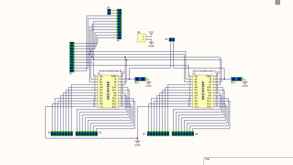

OK, so how about the other version of this price module?
Let’s have a look at the them as well:
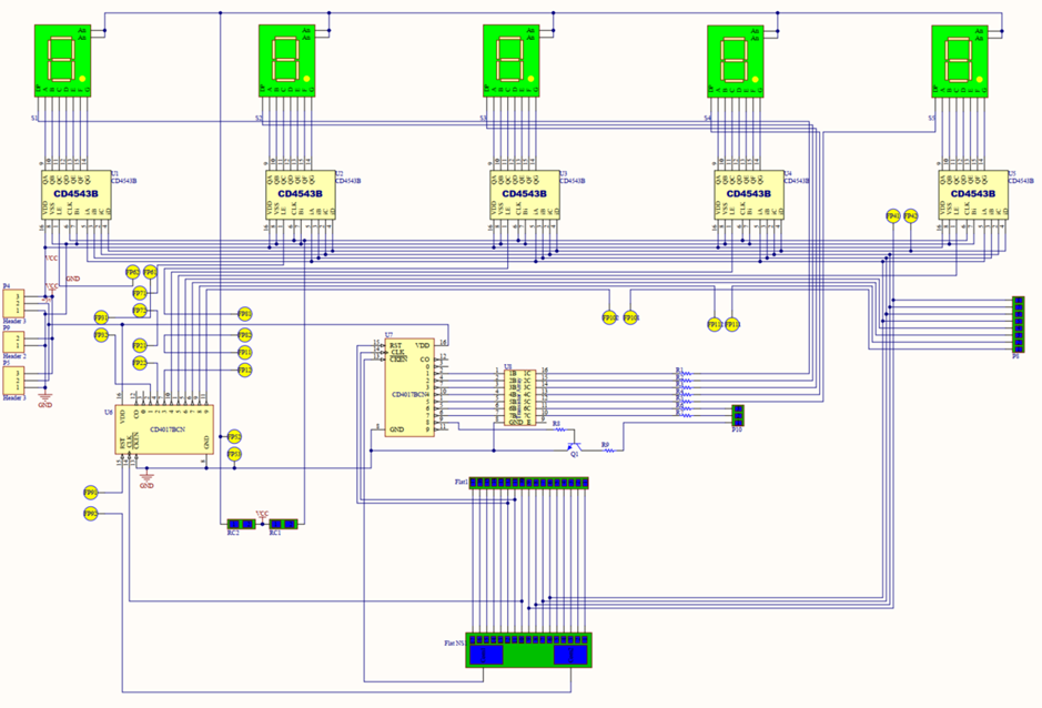

This PCB board is essentially the same as version 2. But it’ s a single sided one. I managed to turn version 2 into a single sided board by rearranging the chips a little bit here and there. You might notice a few more jumpers in the schematic (the yellow dots). that is because this is a single sided board of course and anything that exists on the board, should be on the schematic too. That’s how the routing on the PCB becomes easier. Because all of the connections will be visible.
The PCB is designed in such a way that it could accommodate both common anode and common cathode 7-segments. You could just solder a few pads together and the board is set to function with either type. That is because CD4543s can handle both type of seven segments (comm. A and comm. K). the CD4017 however, has positive outputs. it’s outputs only go HIGH. that would make it incompatible with common Anode 7-segments. To solve that issue, I have included a transistor array that would reverse it’s output from positive to negative for display the decimals. That way, if the 7-segments are the common Anode, we’ll just install an extra transistor array and it’s all good. If it’s the common Cathode 7-segment, we’ll just use jumpers instead of a transistor array chip. Pretty neat right?
Let’s see the other 2 version left. for a smaller and larger than 5x7 seven segment:
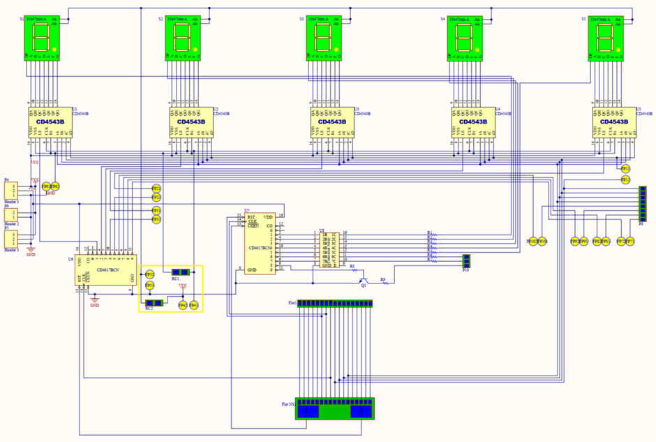
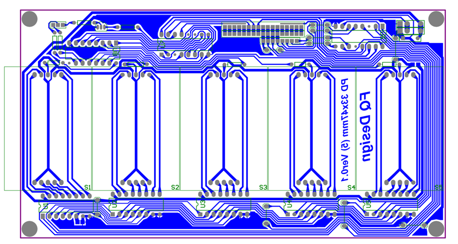
You can see the PCB for the 33x47mm 7-segments looks a bit more congested. It’s not more congested actually. it’s just that the 7-segments are smaller in here.
I did some housekeeping on the I/O part of things as well. so the board has a neat I/O.

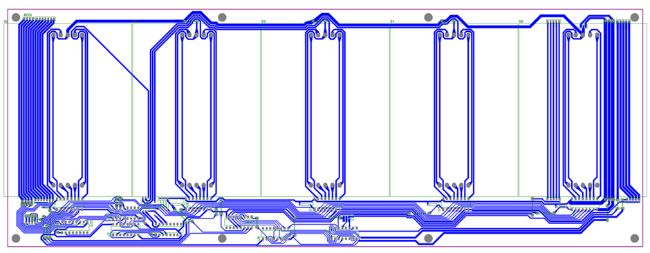
This display module was quite an interesting one because it housed the largest type of seven segment that I would use for this project. the 90 x 120mm size of 7-segments which can be clearly seen from 30 meters away. I don’t really know why someone would use this size. Unless they want to install it close to the ceiling for everyone to see. Anyhow, before I would receive the order for this, I had thought about it and designed it to be ready.
I realized that because the seven segments are quite large, then the wiring for this would get long. That means that the BCD line might become unreadable at the 10th price or more. So I built in a sort of a repeater if you will that will help to revitalize the BCD signal for the modes that are installed after this one. I used the CD4009 chip. It’s a CMOS Hex Buffer/Converter. You can download the datasheet here.
Alright! We’ve covered all of the PCB and Schematic designs for this project. Let’s move on to the coding!
6. What’s In the Code?
I used the “PIC Basic Pro” language to code this display. The coding for this project didn’t take long (3 months). Because it didn’t include too many different chips and I was using an easy language. It was a streamlined design across all modules and therefore the code could easily be copied or written in accessible in blocks that can be called by “GOSUB”s. Changing a few numbers in code would allow you to install less or more price modules. That easy.
You can download the entire code here. Since this was my first coding project back when I was 19, some parts of it might look a little similar to spaghetti code… :) . It was a good starting point for me though and the code functional and error-free. I tried not to use the GOTO syntax as it would break the code’s flow. So the MAIN of the code connected to basically most of the other GOSUBs.
In this section, we will talk about:
The Global Configuration.
Writing Code Into CD4543 7-Segment Driver Chip Using CD4017 Decade Counter.
Writing and Reading Data From the Microcontroller’s EEPROM For Remembering Prices.
How the Animation Mode Is Coded (Blinking Prices)
THE GLOBAL CONFIGURATION
Configuring the code correctly on top of the program allows for less debugging later on during your coding session. For instance, you can set the ports and their specific pins to be an either input or output in the beginning with Tris register (i.e. TrisA for portA, TrisB for portB & so on). Therefore, you won’t have issues with a pin’s I/O settings when sending commands to it.
There are other settings in a code that are of importance as well. For instance, you will need to set the type of Variables that you’re using with the var syntax (Are they a Byte? a Word? a Long?) as well as Oscillator frequency that the microcontroller is running on and etc.

Including modedefs.bas will be necessary for communication with other chips (if any) and including alldigital.php will help to keep all of your ports in digital mode (keep the chip’s built-in DACs off) if you don’t use the DACs (Digital to Analog Converters). This is because the analog modules are sometimes turned on by default in the chip’s fuse bits. So you might be scratching your head for hours, wondering why your port doesn’t function well. The reason could be this setting that hasn’t been set correctly.
If you wish to keep some of the ports in digital mode and some others in analog mode, then you’ll have to read the datasheet to figure out what is the right register name to use that will manipulate the intended fuse bits in charge of this. For example in the chip that I had used for this project (PIC16F877a), setting ADCON1 = #00000111 would turn off the internal DAC (analog module) and keep the ports in Digital mode (as can be seen in the picture). I had used the alldigital.php, but I thought I would throw register in as well just for good measure.
Another helpful register is TRIS. This register can help you to set a whole port or it’s specific pins to either an input or an output. You can see in the configuration above that I’ve set TrisA = $11000000. This will keep two of the pins as inputs in port A and the rest of them will act as an output. In some micrcontrollers, there are internal pull up or pull down resistors that you can activate using the correct port register. So you can reduce the number of components you’d use for your design and still read your input port correctly (because of the pull up or pull down resistors).
WRITING CODE INTO CD4543 7-SEGMENT DRIVER CHIP USING CD4017 DECADE COUNTER.
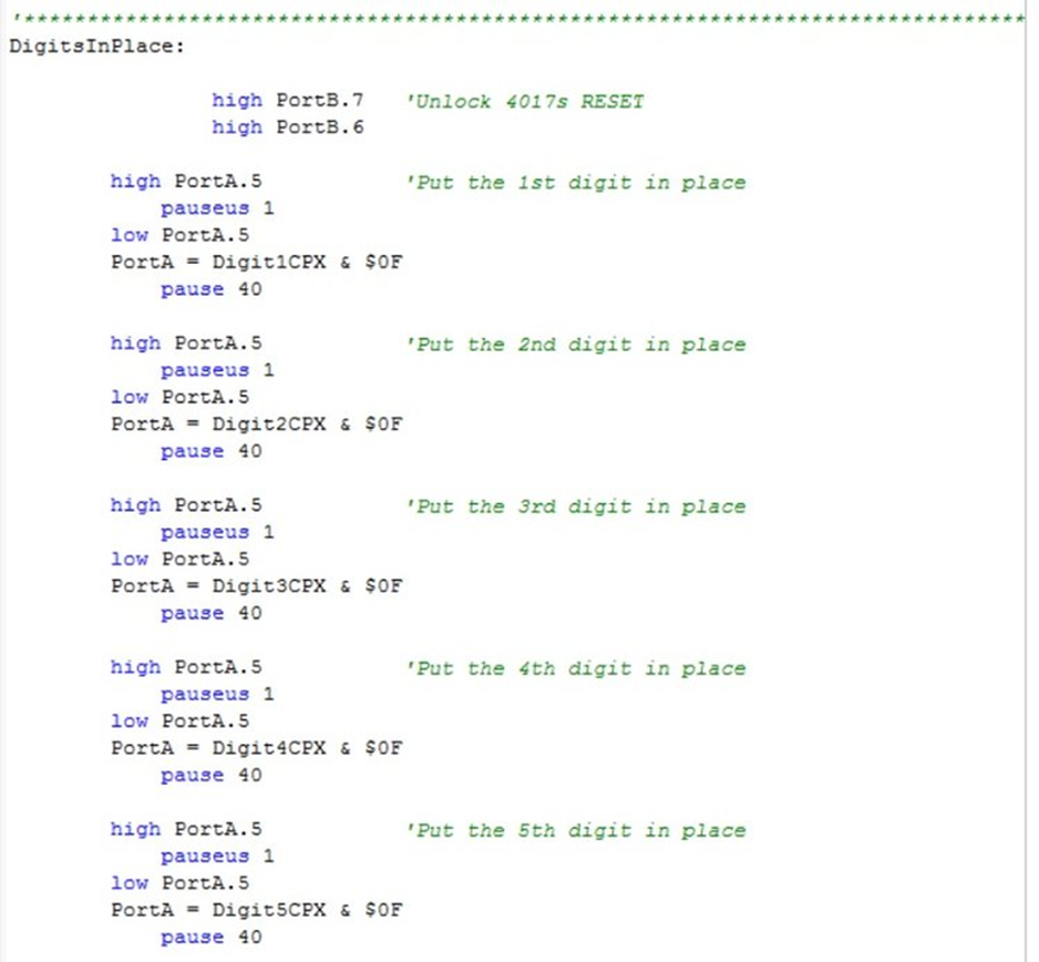
As you can see in the source code here, The first thing this SUB “DigitsInPlace” does is to unlock the RESET pins of the CD4017. Then, it will toggle the pin that is connected to the clock of our CD4017. In this case PortA.5. By doing so, the CD4017 decade counter will count one. And with every count, it will be activating the latch of the previous CD4543 and disabling the latch of the next one. Because when the latch is disabled, you can write a digit to the chip. When it’s enabled, you can’t write anything.
By doing so, with every clock toggle on PortA.5, we have the opportunity to change the value of one digit in our set up. Starting from left to right.
If you’ve noticed, Port A is both responsible for sending the clock signal and the digit value to the BCD. How can it do both? well, by adding “& $0F” to our variable in the code. “& $0F” will help to send 4 digits to our port and truncate the remaining numbers in a binary value. The code above is using the same trick. i.e. ‘PortA = Digit1CPX & $0F”. That will help to send only a BCD value out of Digit1CPX to our PortA. This is actually due to lack of Nibbles (half a byte is called Nibble) in PICBasic Pro. You can’t assign a variable as a “Nibble”. So you’d have to resort to other ways of sending 4 bits to your port.
WRITING AND READING DATA FROM THE MICROCONTROLLER’S EEPROM FOR REMEMBERING PRICES.
This is probably the easiest part of code in PIC Basic Pro. In order to write a value into your chip’s EEPROM, you can just use the WRITE command followed by a number which is the EEPROM that you wish to write to.

In this part of the code, you can see that the ‘DisplayCount’ Variable will determine which EEPROM bytes need to be updated according to the display that is being set. And then it will write the digit that is being shown to the appropriate EEPROM byte (memory address). For example, Byte 1 to 5 are for the first price. Byte 6 to 10 are for the second price and so on. I decided to store the value of the decimal into another byte. Reading the data is very similar. You can use the READ command in a similar writing and the get value in your variable.
One might say that this isn’t an efficient way of coding your digits and that I should’ve used a LONG to represent all 5 digits (Maximum is 99,999 for 5 digits. LONG can handle 4294967295). Well, sure I could. but that would still take 4 bytes of my EEPROM (a LONG has 4 bytes in it) for a 5 digit number and introduced conversions when reading, writing & displaying the data on the BCD. Here I’ve used 6 bytes (one for decimal), but I’ve achieved the same results without making the code very complicated. This code is simple. So if you wish to add more prices or remove some, it’s very easy to modify. If there were more digits for each price though, using a LONG could’ve been more efficient for sure.
HOW THE ANIMATION MODE IS CODED (BLINKING PRICES).
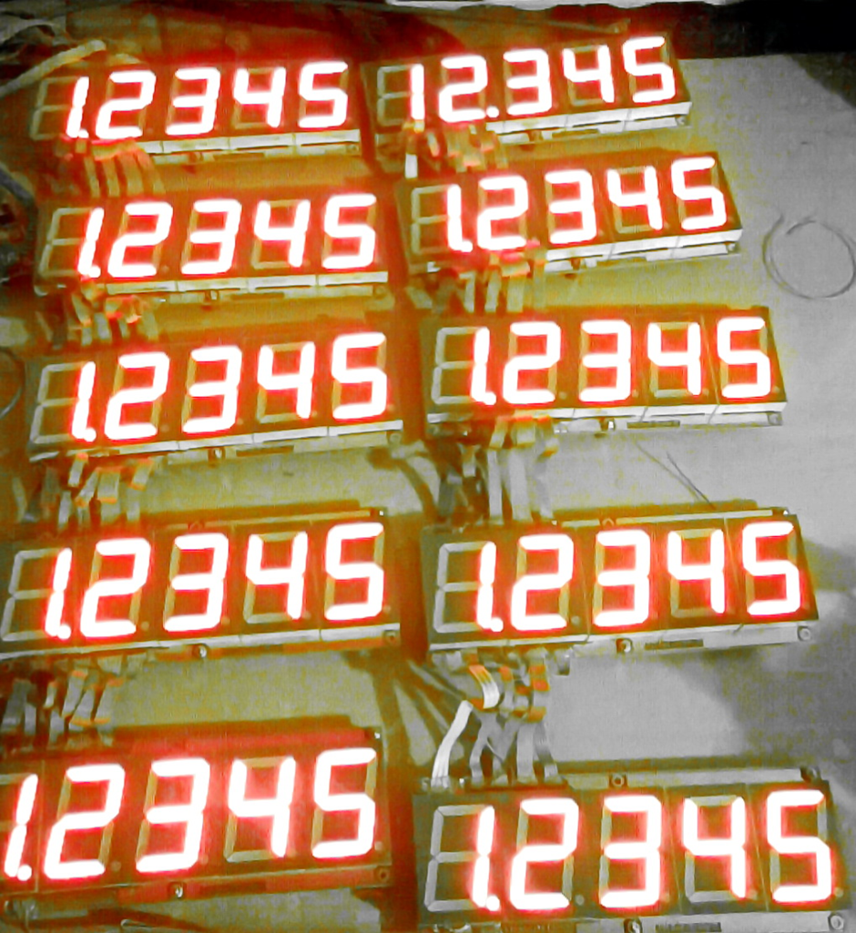
The animation mode is possible thanks to the behavior of our 7-segment driver chips “CD4543”. These chips will show a number when they have a BCD input from 0 to 9. But they will show nothing if the input is number 15. So by taking advantage of this, we can turn the digits on and off. And if it’s done in sequence with some PAUSEs in between, then you’ll see the digits shifting to left and right. Or maybe the whole panel toggle between on and off to catch people’s attention.
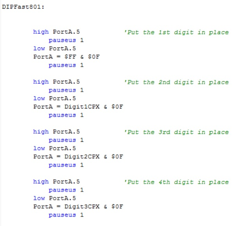
In the image above, you can see that “PortA = $FF & $0F”. So we’re essentially sending $FF which is 15 to our BCD line. This will turn off the first digit. We would then PAUSE for about 200ms and go to another SUB:
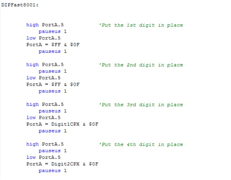
Now in this image above, we see that 2 digits are shifted. Because we’re loading two of the CD4543s with $FF. We could then PAUSE for 200ms and proceed with the third SUB. Actually, this part of the code can be summarized further with a few commands as well.
This can go on and on until all of the digits are shifted to left or right depending on where we start from. We can also load all of the CD4543s with $FF and turn off the whole panel:

As you can see, this will turn off the whole display. Setting the appropriate digits will turn the display back on. Pretty simple right? That’s what I thought.

7. Final Words.
This project helped me get familiar with designing PCBs and learn more about coding in PIC Basic Pro. I sold a few units. But my clock project was more successful as there was less competition for it in the market compared to these Forex displays that many people were producing.
Some parts of the code could’ve been written more efficiently. But well, I was just starting to code and I’d say it wasn’t bad for a 19 year old.
It was the first time for me to print PCBs. They came out pretty well without any flaws and worked straight away without the need for any modifications (I didn’t print a test PCB).
It’s a modular design and even today, 10 years later, it’s modules are easily integrable into other projects. If I wanted to update this project, I would probably write an API for it to connect to a raspberry Pi of some sort (maybe Pi zero) so it can update the prices automatically with a wifi connection.
So was it worth it? to spend nearly 4 months developing this project? heck yeah! That’s how it is done! That’s how you learn Electronics! I do encourage you to do the same. Projects, projects and more projects. Think of it as something you’d want to sell. Something market-ready. Iron all of the flaws. Then, it’ll become a very interesting project and maybe a good product ;)
If you liked this blog, please show some love and share it with your like-minded friends. It’ll motivate me to write more.
Thank you.


Comments